Informative Links
- Test Fixture and MEMS Test Fixture Design
- Circuit Design
- Semiconductor Fab Equipment Design
- Instrument Design for the Chemical, Biotech and Life Sciences Industry
Portfolio of
Example Projects

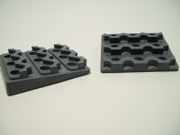
Jig for high temp brazing of Cu-Mo transistor headers

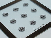
Chrome mask for special processing of Si die.
Semiconductor Fabrication Equipment Design
Semiconductor fabrication and packaging equipment for non-mainstream applications such as MEMS fabrication, compound semiconductor components such as LEDs, and other unusual devices often requires a solution that is custom designed. We have designed numerous solutions for both silicon and compound semiconductor fabrication processes. Our strength and ability to provide a practical solution comes partly from our knowledge of microelectronics, experience working in semiconductor fabs, and our innovative mechanical design skills.
Some examples of some of our projects:
- Modify wafer probers to allow optical measurements
- Designing jigs and special soldering equipment for creating void free die attachment of large devices.
- Making custom modifications to existing and off the shelf semiconductor fab equipment.
- Design of jigs and fixtures to facilitate special and nonstandard packaging techniques.
- Designing photomasks for unusual semiconductor fab processes.
- Reworking and redesigning semiconductor fabrication equipment to make it suitable for special applications.
Also, one advantage we have when working on these types of projects is our in-house machine shop. When machining modifications and/or adding features to existing fab equipment which is clean and dust free, we can often preserve the clean state since we are doing the machining ourselves. This can save a lot of time since tearing down a machine, sending parts out for machining, cleaning, and then reassembling can be costly, time consuming, and sometimes not possible at all.