Informative Links
- Test Fixture and MEMS Test Fixture Design
- Circuit Design
- Semiconductor Fab Equipment Design
- Instrument Design for the Chemical, Biotech and Life Sciences Industry
Portfolio of
Example Projects
Custom Semiconductor Fabrication Equipment Examples
Shown below are some pictures of tooling components used in the manufacture of high voltage transistors. These are good examples of the variety of skills we can apply to create a solution for your application. The transistors were part of an old product line and most of the associated fab equipment was custom designed. The parts shown below were part of a project to correct and improve several different deficiencies in the fab process and collectively increased the yield by as much as 30%. The design involved creatively applying multiple skills such as photomask design, working with machinable ceramics, photo etching and silver brazing. This is another example of a project where good mechanical skills combined with electronic skills (knowledge of microelectronic processes) were necessary for a creative unique solution.
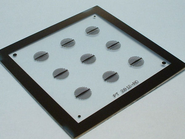
Special chrome mask designed for use with a photoresist process on individual Si die.
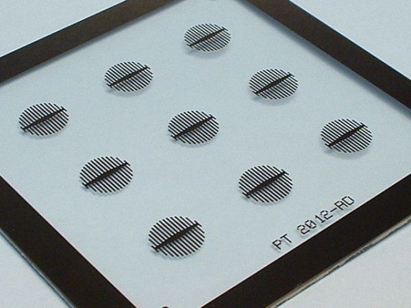
Close up view of mask. Special geometry of features was designed in AutoCAD.
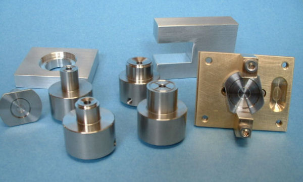
Components including wafer chucks custom designed to enhance a special process for cutting Si wafers. All machining was done at Henning Engineering to save time and allow custom in-house machining and modification of the original piece of equipment.
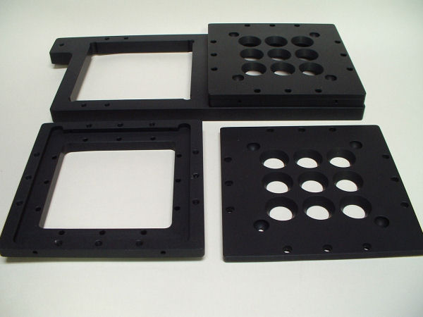
Jig for custom alignment of Si die and photomask.
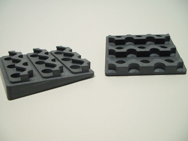
Special jig designed for void free silver brazing of Cu-Mo headers for transistors. Jig is made of machinable ceramic and designed to work at temperatures of up to 1100 ºC.